eltonlaw sundries
Building a Grow Box Part 1 - STM32 basics: Getting to blinky with CMSIS
2024-06-16 01:19AMI've been using the STM32CubeIDE to build and flash the firmware, it's not bad and it works but I have a few issues. Why doesn't flashing the device have a keyboard shortcut? As a former front end developer I need to click this button every 10 seconds or I'll die. Hot reloading and access to a REPL have ruined me. There are other quality of life issues I have, but these could possibly be chalked up to user error since I'm a crusty fart about Vim and half my brain is permanently occupied by keybindings. The IDE doesn't run on my laptop for some reason (possibly an incompatibility with Wayland). I don't like the idea of tying the build process to closely to the IDE because then the repo is a lot more dependent on the local system and CI is hard to setup. I'm not sure what's happening to the code during the build process.
So I decided to build a simpler project with just Make and the ST provided CMSIS for the G070. CMSIS (Cortex Microcontroller Software Interface Standard) is a vendor-independent hardware abstraction layer for the ARM Cortex processor series. You can't simply use the code for one processor for some other processor but there are standardized software APIs for system initialization and configuration and so on. Interactions with the CPU will be through bit twiddling registers. I like reading datasheets, makes me feel like a real engineer.
The STM32G070RB is a 32-bit Cortex M0+ CPU which means it implements the ARMv6-M instruction set, this is not the same as the ARMv6 Thumb instruction set though they are closely aligned. To start, we'll build and flash a simple blinky using the built-in LED on the Nucleo dev board I'm working with. At a high level:
- Hook up a cross compilation toolchain into Make
- Compile some code that does the following:
- Initialize the system clock, we'll need it to implement the equivalent of
time.sleep(ms: int) - Initialize the GPIO peripherals being used
- Configure the pin the LED is connected to for output (from the schematic, GPIO PORT A, PIN5)
- Loop forever: toggle pin, wait 1 second
- Initialize the system clock, we'll need it to implement the equivalent of
- Flash to device
Cross-compiling and linking the binary
Grab the CMSIS files:
git submodule add git@github.com:STMicroelectronics/STM32CubeG0.git
It's a standard C compile, but using the ARM toolchain:
CC=arm-none-eabi-gcc
CFLAGS=-mcpu=cortex-m0plus -mthumb -g -O0
CFLAGS+=-I./STM32CubeG0/Drivers/CMSIS/Device/ST/STM32G0xx/Include
CFLAGS+=-I./STM32CubeG0/Drivers/CMSIS/Include
CFLAGS+=-I./src
LDFLAGS=-Tlinker_script.ld -nostartfiles
OBJCOPY=arm-none-eabi-objcopy

SRC = $(wildcard src/*.c)

all: main.bin

main.bin: main.elf
	$(OBJCOPY) -O binary $< $@

main.elf: $(SRC)
	$(CC) $(CFLAGS) $(LDFLAGS) $^ -o $@

clean:
	rm -f *.elf *.bin

flash: main.bin
	STM32_Programmer_CLI -c port=SWD -w main.bin 0x8000000 -rst
The flash recipe at the end writes the final binary file to where flash memory starts on the processor (found in the datasheet). The processor is connected to an intermediary device (ST-LINK) by two pins SWCLK (serial wire clock) and SWDIO (serial wire data I/O), this is a debug interface called SWD. This intermediary device bridges SWD to USB-B and that's what talks to the STM32_Programmer_CLI
The source file src/main.c will just be a no-op for now.
#define STM32G070xx
#include "stm32g0xx.h"

int main(void) {
    while (1) { }
}
#define STM32G070xx is needed because #include "stm32g0xx.h" is a wrapper header file for the the entire G0 family, including the processor-specific headers only when the a processor specific define exists. Adding #define STM32G070xx links in STM32CubeG0/Drivers/CMSIS/Device/ST/STM32G0xx/Include/stm32g070xx.h (from the CMSIS git submodule earlier) which has all the register and bit definitions, address mappings and structs needed to use the peripherals. This way we don't have to write binary directly, but can bit bang with definitions.
Stepping through the program
On-chip debugging is a way to run, pause and inspect the state of the hardware as your code runs. As mentioned previously, the STM32G070 has a SWD interface, providing the pins SWDIO and SWCLK. The nucleo board I'm using has an ST-LINK interface on it, a separate chip, which is what manages the USB connection to the computer. This is physically wired to the SWDIO and SWCLK on the microcontroller and USB commands are converted to the appropriate signals on those pins.
In practise, OpenOCD starts a server that connects to the microcontroller and client programs (GDB, telnet or TCL) control the microcontroller through it. The server needs to be configured so it can properly send and receive data but there's a bunch of standard configurations provided on GitHub, so after cloning that repo, starting the OpenOCD server, for my setup:
openocd -f interface/stlink.cfg -f target/stm32g0x.cfg -s $(pwd)/openocd/tcl
Start a GDB server
arm-none-eabi-gdb main.elf
Connect GDB server to OpenOCD server, and load the program.
target remote :3333
load
monitor halt
monitor reset init
Testing the connection with:
int main(void) {
    int x;
    while (1) {
        x = add(x, 3);
    }
}
...And stepping through it shows x += 3 each loop indicating the code has compiled and flashed correctly!
(gdb) break main
Breakpoint 1 at 0x800010e: file src/main.c, line 19.
Note: automatically using hardware breakpoints for read-only addresses.
(gdb) continue
Continuing.

Breakpoint 1, main () at src/main.c:19
19          int x = 0;
(gdb) step
halted: PC: 0x08000110
halted: PC: 0x08000112
21              x = add(x, 3);
(gdb) step
halted: PC: 0x08000114
halted: PC: 0x08000116
halted: PC: 0x08000118
halted: PC: 0x08000248
add (a=0, b=3) at src/gpio.c:2
2               return a + b;
(gdb) step
halted: PC: 0x08000254
halted: PC: 0x08000256
halted: PC: 0x08000258
3       }
(gdb) step
halted: PC: 0x0800025a
halted: PC: 0x0800025c
halted: PC: 0x0800025e
halted: PC: 0x0800011c
halted: PC: 0x0800011e
halted: PC: 0x08000120
halted: PC: 0x08000112
halted: PC: 0x08000114
halted: PC: 0x08000116
halted: PC: 0x08000118
halted: PC: 0x08000248
add (a=3, b=3) at src/gpio.c:2
2               return a + b;
With each step, the accumulator var a is increasing by 3, as expected, so we have some C code properly executing additions on the chip now. To interact with the physical world, we'll need a little more setup.
ARMv6-M
Initializing the System Clock
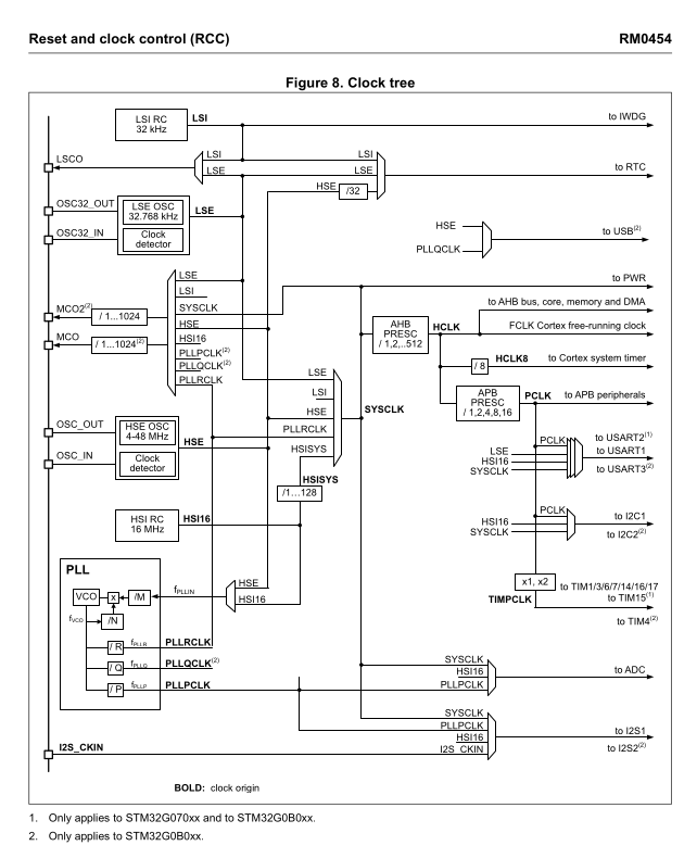
The primary clock source can be set as one of HSI16 RC (high speed integrated 16Mhz), HSE OSC (high speed external clock source), LSI RC (low speed integrated 32Khz), LSE OSC (low speed external clock source), I2S_CKIN (I2S1 peripheral).
Based on whichever one is picked, that becomes the base and affects all the secondary clock signals that derive from it with some prescale divider.
Upon system reset, the HSISYS clock derived from HSI16 oscillator is selected as system clock.
By default, the base processor clock is set at 16MHz. In the CMSIS, RCC (Reset and Clock Control) is what manages system and peripheral clocks. These are all the registers avaialable, they each map to some physical entity in the hardware:
/**
  * @brief Reset and Clock Control
  */
typedef struct
{
  __IO uint32_t CR;          /*!< RCC Clock Sources Control Register,                                     Address offset: 0x00 */
  __IO uint32_t ICSCR;       /*!< RCC Internal Clock Sources Calibration Register,                        Address offset: 0x04 */
  __IO uint32_t CFGR;        /*!< RCC Regulated Domain Clocks Configuration Register,                     Address offset: 0x08 */
  __IO uint32_t PLLCFGR;     /*!< RCC System PLL configuration Register,                                  Address offset: 0x0C */
  __IO uint32_t RESERVED0;   /*!< Reserved,                                                               Address offset: 0x10 */
  __IO uint32_t RESERVED1;   /*!< Reserved,                                                               Address offset: 0x14 */
  __IO uint32_t CIER;        /*!< RCC Clock Interrupt Enable Register,                                    Address offset: 0x18 */
  __IO uint32_t CIFR;        /*!< RCC Clock Interrupt Flag Register,                                      Address offset: 0x1C */
  __IO uint32_t CICR;        /*!< RCC Clock Interrupt Clear Register,                                     Address offset: 0x20 */
  __IO uint32_t IOPRSTR;     /*!< RCC IO port reset register,                                             Address offset: 0x24 */
  __IO uint32_t AHBRSTR;     /*!< RCC AHB peripherals reset register,                                     Address offset: 0x28 */
  __IO uint32_t APBRSTR1;    /*!< RCC APB peripherals reset register 1,                                   Address offset: 0x2C */
  __IO uint32_t APBRSTR2;    /*!< RCC APB peripherals reset register 2,                                   Address offset: 0x30 */
  __IO uint32_t IOPENR;      /*!< RCC IO port enable register,                                            Address offset: 0x34 */
  __IO uint32_t AHBENR;      /*!< RCC AHB peripherals clock enable register,                              Address offset: 0x38 */
  __IO uint32_t APBENR1;     /*!< RCC APB peripherals clock enable register1,                             Address offset: 0x3C */
  __IO uint32_t APBENR2;     /*!< RCC APB peripherals clock enable register2,                             Address offset: 0x40 */
  __IO uint32_t IOPSMENR;    /*!< RCC IO port clocks enable in sleep mode register,                       Address offset: 0x44 */
  __IO uint32_t AHBSMENR;    /*!< RCC AHB peripheral clocks enable in sleep mode register,                Address offset: 0x48 */
  __IO uint32_t APBSMENR1;   /*!< RCC APB peripheral clocks enable in sleep mode register1,               Address offset: 0x4C */
  __IO uint32_t APBSMENR2;   /*!< RCC APB peripheral clocks enable in sleep mode register2,               Address offset: 0x50 */
  __IO uint32_t CCIPR;       /*!< RCC Peripherals Independent Clocks Configuration Register,              Address offset: 0x54 */
  __IO uint32_t RESERVED2;   /*!< Reserved,                                                               Address offset: 0x58 */
  __IO uint32_t BDCR;        /*!< RCC Backup Domain Control Register,                                     Address offset: 0x5C */
  __IO uint32_t CSR;         /*!< RCC Unregulated Domain Clock Control and Status Register,               Address offset: 0x60 */
} RCC_TypeDef;
SysTick is a standard component of the ARM Cortex-M cores and can be used for context switching or implementing sleep/delay functions among other things. It is a 24-bit clear-on-write timer that has some initial value and decrements every clock cycle. When it hits 0 it'll generate a SysTick interrupt. There's a provided function for configuring this already:
__STATIC_INLINE uint32_t SysTick_Config(uint32_t ticks)
{
  if ((ticks - 1UL) > SysTick_LOAD_RELOAD_Msk)
  {
    return (1UL);                                                   /* Reload value impossible */
  }

  SysTick->LOAD  = (uint32_t)(ticks - 1UL);                         /* set reload register */
  NVIC_SetPriority (SysTick_IRQn, (1UL << __NVIC_PRIO_BITS) - 1UL); /* set Priority for Systick Interrupt */
  SysTick->VAL   = 0UL;                                             /* Load the SysTick Counter Value */
  SysTick->CTRL  = SysTick_CTRL_CLKSOURCE_Msk |
                   SysTick_CTRL_TICKINT_Msk   |
                   SysTick_CTRL_ENABLE_Msk;                         /* Enable SysTick IRQ and SysTick Timer */
  return (0UL);                                                     /* Function successful */
}
ticksis the number of clock ticks per interrupt.SysTick->VALis the tick counter and it gets set to 0 so that we're at known state.SysTick_CTRL_TICKINT_Mskis a uint32 with just the bit that enables the SysTick interrupt set to 1SysTick_CTRL_ENABLE_Mskis a uint32 with just the bit that enables decrementingSysTick->VALSysTick_CTRL_CLKSOURCE_Mskis a uint32 with just the bit that sets the processor clock as source for the SysTick timer- Oddly in the ST provided HAL, there's a
__weak HAL_StatusTypeDef HAL_InitTick(uint32_t TickPriority)called as part ofHAL_StatusTypeDef HAL_Init(void)and it's passing in#define TICK_INT_PRIORITY 0U, setting it to 0 (highest priority) whereas CMSIS is setting it as 3 (lowest priority, it's a 2 bit value). So as is, SysTick stuff will be less accurate if there's a lot of higher priority interrupts generated. I'll leave it as is for now.
Earlier, we saw that the processor clock was set at 16 MHz and 16MHz is 16 million cycles per second, 1ms is 0.001 seconds, therefore 16000 cycles would be 1ms. So to setup SysTick for 1ms per tick:
SysTick_Config(16000);
SystemCoreClockUpdate();
We need to call SystemCoreClockUpdate because SysTick_Config only changes the register values but SystemCoreClockUpdate() ensures that the global variable SystemCoreClock is updated to reflect the current core clock frequency.
One last thing, when enabling interrupts, it's important to define their associated handlers. From the device specific startup.s file, all interrupts handlers are declared as weak symbols that default to a Default_Handler which is a no-op infinite loop.
...
.global Default_Handler

  ...
  .section .text.Default_Handler,"ax",%progbits
Default_Handler:
Infinite_Loop:
  b Infinite_Loop
  .size Default_Handler, .-Default_Handler

  ...
  .weak      SysTick_Handler
  .thumb_set SysTick_Handler,Default_Handler
So if SysTick is enabled and generates an interrupt without a definitive definition of SysTick_Handler, it'll hang forever. Since we've configured it to hit 0 every 1ms, simply incrementing a number every interrupt counts the milliseconds since initialization.
volatile uint32_t uw_tick = 0;

void SysTick_Handler(void) {
    uw_tick++;
}
At a rate of a tick per 1 ms, it'll only overflow after 2^32 or 4,294,967,296 ms (~49.71 days). Overflow will be handled later, but since this code will be called in such a tight loop, logic will instead be put into everything that uses uw_tick.
GPIO configuration
On the nucleo board, there's a green LED, LD4 connected to PA5.
To get that to blink, the GPIO pin needs to be configured for output. All peripherals are disabled by default, so first the GPIO clock needs to be enabled, this is managed by RCC.
RCC->IOPENR |= RCC_IOPENR_GPIOAEN;
/* Ensure clock is enabled by read op */
volatile uint32_t tmpreg = RCC->IOPENR & RCC_IOPENR_GPIOAEN;
(void) tmpreg; /* avoid compiler warnings about unused var */
The relevant global struct that deals with that is GPIOA defined in STM32CubeG0/Drivers/CMSIS/Device/ST/STM32G0xx/Include/stm32g070xx.h
#define GPIOA               ((GPIO_TypeDef *) GPIOA_BASE)
...
/**
  * @brief General Purpose I/O
  */
typedef struct
{
  __IO uint32_t MODER;       /*!< GPIO port mode register,               Address offset: 0x00      */
  __IO uint32_t OTYPER;      /*!< GPIO port output type register,        Address offset: 0x04      */
  __IO uint32_t OSPEEDR;     /*!< GPIO port output speed register,       Address offset: 0x08      */
  __IO uint32_t PUPDR;       /*!< GPIO port pull-up/pull-down register,  Address offset: 0x0C      */
  __IO uint32_t IDR;         /*!< GPIO port input data register,         Address offset: 0x10      */
  __IO uint32_t ODR;         /*!< GPIO port output data register,        Address offset: 0x14      */
  __IO uint32_t BSRR;        /*!< GPIO port bit set/reset  register,     Address offset: 0x18      */
  __IO uint32_t LCKR;        /*!< GPIO port configuration lock register, Address offset: 0x1C      */
  __IO uint32_t AFR[2];      /*!< GPIO alternate function registers,     Address offset: 0x20-0x24 */
  __IO uint32_t BRR;         /*!< GPIO Bit Reset register,               Address offset: 0x28      */
} GPIO_TypeDef;
And a basic output configuration for Port A, Pin 5:
/* Configure pin to be output */
GPIOA->MODER &= ~GPIO_MODER_MODE5;
GPIOA->MODER |= GPIO_MODER_MODE5_0;

/* Clear pin to make pin push-pull mode (as opposed to open drain) */
GPIOA->OTYPER &= ~GPIO_OTYPER_OT5;

/* GPIO_OSPEEDR_OSPEED5_0 corresponds to `01` in bit[10:11] of OSPEEDR which means "Low speed"  */
GPIOA->OSPEEDR &= ~GPIO_OSPEEDR_OSPEED5;
GPIOA->OSPEEDR |= GPIO_OSPEEDR_OSPEED5_0;

/* Clears the pin5 bits in PUPDR which means no pull-up or pull-down */
GPIOA->PUPDR &= ~GPIO_PUPDR_PUPD5;
Once we have this configured, we can run the following in an infinite loop to set pin 5 for a second, clear it for a second
while (1) {
    GPIOA->BSRR = GPIO_BSRR_BS5;
    delay(1000);
    GPIOA->BSRR = GPIO_BSRR_BR5;
    delay(1000);
}
and that blinks the light: